A power and ground backplane to simplify IoT component connectivity
IoT projects are fun until you move them off the breadboard and then have to solder create reliable connections and power and ground connections. Some people solder some people use small super-cheap breadboards. I tend to use jumper wires and connectors because most of my stuff is a one-off or super-small batch. It makes rework easy and reliable. The downside is that connectors take up space. The rest of this demonstrates a simple way of making this happen.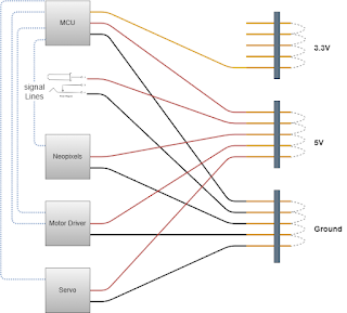
Power (5V) is injected at the jack. There are power and ground connectors for each device that requires power or ground.
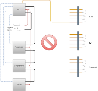 Connections should be as direct as possible. Don't create loops. Don't route ground through a device to a different pin to another device.

Video
Schematic

Three sets of headers are soldered to a breadboard and joined to each other jin banks.
Power (5V) and ground lines run from each device and from the jack to the distribution connectors which are plugged into the headers.
3.3 Volt is not on the jack. It is supplied from a voltage regulator on the board and available on its own header row. It is supplied in the schematic from a voltage regulator on board the CPU/MCU and not from the external power jack or USB
Tie everything back to the same source

Power Distribution

Sometimes I twist them all together wire-tie style and solder that bundle. The bundle doesn't take up a lot of space and provides a reliable connection. Then I'll shrink-wrap the solder point to avoid shorts
Here I built a power distribution hub.

All the single power and ground lines are point-to-point with only one pin-to-pin cable. Power and Ground run from the central location to every device. I like to chain all of the components directly back to the same ground point. This means there is always an N-Way connection to all N devices for both power and ground.
Another approach is to make small power and ground connector banks out of protoboard and connector pins. The picture at the right has 3 banks intended for ground, 3.3V, and 5V. The connector on the right is bigger than the connecter set because I knew I'd have to add another later by adding another pin.
All the right-angle pins were soldered to the protoboard on the copper side. Then I ran a bare wire across all the pins in a bank and soldered the wire to the pins.Concerns
- Connectors take up a lot more space than direct wire soldering.
- The back of the protoboard should be covered in an insulator type of tape.
Revision History
Created 2023 02 21


Comments
Post a Comment